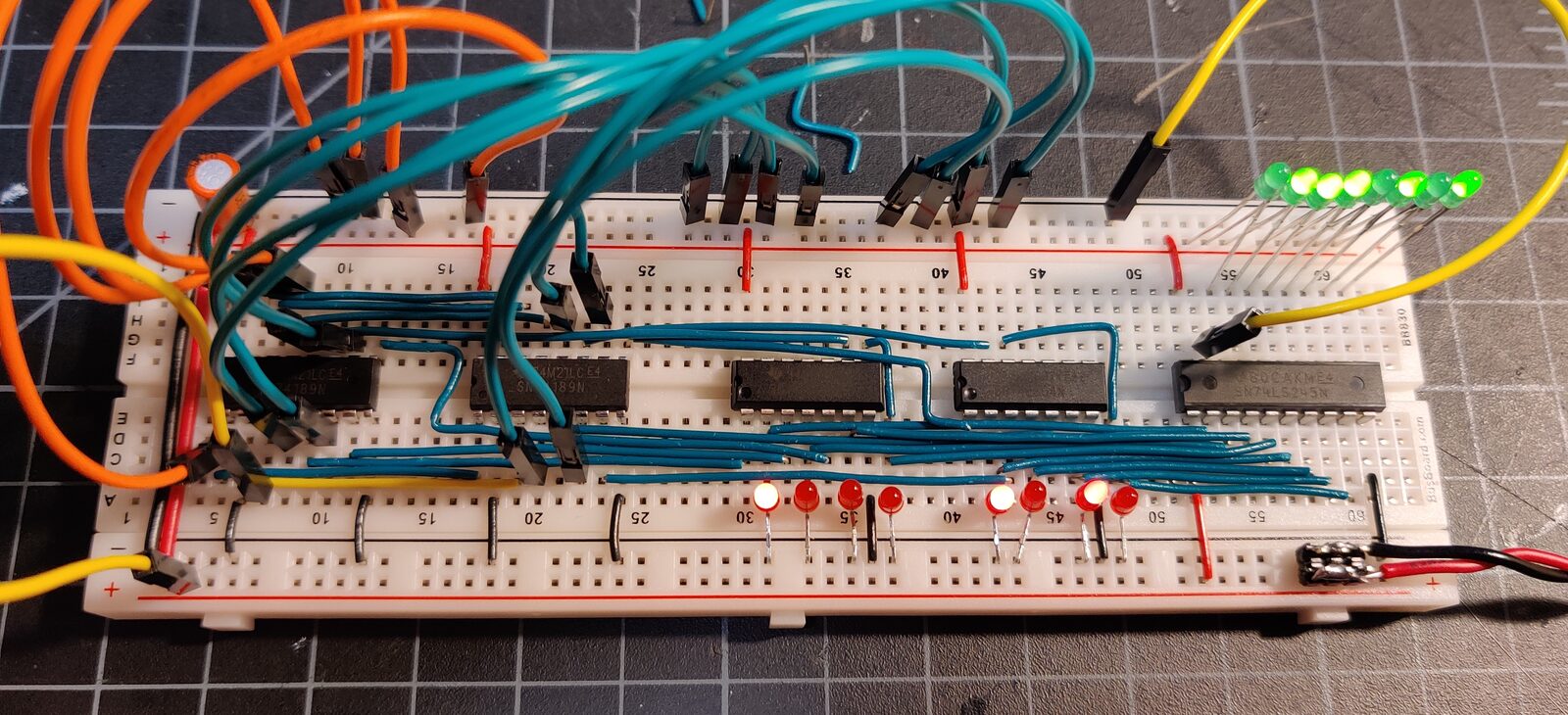
I built an 8-bit computer from scratch on breadboards. Not a microcontroller, not an emulator, an actual CPU wired up gate by gate out of a pile of 74-series logic chips. The whole thing sprawls across something like six or seven breadboards by the end, with a rat’s nest of jumper wires connecting everything. It’s the kind of project that looks completely insane sitting on a desk and mostly is.
The idea was to understand what’s actually happening inside a processor at the level where there’s no magic left. So instead of trusting that “the CPU fetches an instruction and executes it,” I built each piece that makes that sentence true and watched the electrons do it.
The design is Ben Eater’s SAP-1, from his breadboard-computer series. Not my architecture; my wiring, my debugging.
The bus and the clock
At the heart of it is an 8-bit bus, which is really just eight wires running the length of the boards that everything talks over. Only one thing is allowed to put data onto the bus at a time, and any number of things can read from it. That single rule is basically the whole architecture. Every module hangs off this bus and has control lines that decide whether it’s driving the bus, reading from it, or sitting quietly.
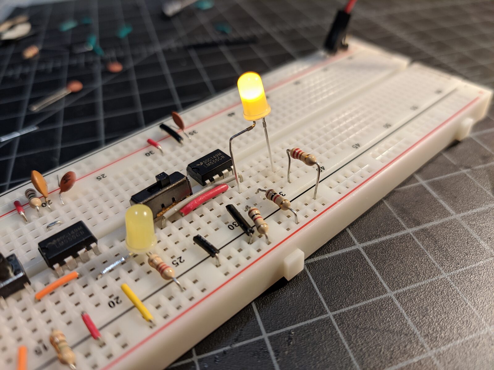
The clock module drives the whole thing. I built it around a couple of 555 timers so I can run it as a steady oscillator or switch to a manual mode where I press a button to advance one tick at a time. There’s a potentiometer to crank the speed up or down. Running it slow and single-stepping is how you actually debug the thing, because you can watch a value crawl from one register onto the bus and into another register one clock edge at a time. Realistically it tops out somewhere in the low hundreds of hertz before the cheap logic starts getting flaky, which tells you something humbling about what “slow” used to mean.
Registers, memory, output
For storage inside the CPU there are two registers, A and B. They’re just latches that grab whatever is on the bus when told to and hold it. The ALU sits between them and does the math. I wired it up out of binary adder chips, and to get subtraction I run the B register through a bank of XOR gates that can flip all the bits, then add one, which is two’s complement. So the same hardware does addition and subtraction depending on one control line. The ALU can also raise a couple of flags, a carry flag and a zero flag, which later let the computer make decisions.
There’s a RAM module with 16 bytes of memory. To address it there’s a separate little register called the memory address register that holds which location you’re pointing at. I put dip switches on it too so I can hand-toggle a program into memory in binary before running it, which is exactly as tedious as it sounds and weirdly satisfying.
The program counter keeps track of which instruction is next. It counts up on its own, but it can also be loaded from the bus, and that load ability is the entire trick behind jumps. A jump instruction just shoves a new value into the program counter and suddenly execution continues somewhere else.
The output is an 8-bit register wired to a 7-segment display so I can actually see numbers come out in decimal. Getting decimal out of a binary value is not free. I burned a lookup table onto an EEPROM that converts the binary value into the right segment patterns, and a little counter rapidly cycles through the four digits fast enough that your eye sees a steady number. It even handles signed values so it’ll show negatives.
The control logic
The part that ties it all together, and the part that took the longest to get right, is the control logic. An instruction is never one action. It’s a short sequence of micro-steps. Fetching an instruction alone takes a few ticks: put the program counter on the bus, load it into the memory address register, read that byte of RAM into the instruction register, bump the counter. Then the actual instruction plays out over a few more steps.
I encoded all of that microcode into a pair of EEPROMs. The instruction register’s top bits and a small step counter feed into the EEPROMs as an address, and what comes out is the control word for that exact moment, sixteen-ish bits that fan out to every enable and load line in the machine. So the “brain” of my CPU is genuinely just a lookup table I programmed. Change the contents of those chips and you change the instruction set. I wrote a little code to generate the EEPROM contents rather than typing thousands of bits by hand, because there’s a limit.
Running it
Once it all worked, I could write tiny programs. The classic one is a loop that counts, or adding two numbers and displaying the result, or a Fibonacci sequence that runs until it overflows the 8 bits and wraps around. Watching it compute Fibonacci on hardware I wired myself, one clock tick at a time, with LEDs blinking down the bus as values move around, is one of those things that permanently changes how you think about every computer you’ll ever touch after that.
Half the project was debugging. A single wire in the wrong hole and the whole thing does something baffling. But that’s also where the actual learning lived. By the end there was nothing left in a CPU that felt like a black box to me, because I’d been elbow deep in every part of it and fixed every part of it at least twice.